Introduction to PCB Design Rules
Printed circuit board (PCB) design is a complex process that requires careful planning and attention to detail to ensure the final product functions as intended. To help avoid common issues and create high-quality PCBs, it’s important to follow a set of established design rules.
In this article, we’ll explore 10 essential PCB design rules that will help you optimize your designs, improve manufacturability, and ultimately create better PCBs. By adhering to these guidelines, you can minimize the risk of errors, reduce costs, and streamline the production process.
Rule 1: Maintain Proper Clearance and Creepage Distances
One of the most critical aspects of PCB design is maintaining appropriate clearance and creepage distances between components, traces, and other conductive elements. Clearance refers to the shortest distance between two conductive parts, while creepage is the shortest path along the surface of the insulating material between two conductive parts.
To ensure proper clearance and creepage distances, consider the following:
– Voltage rating: Higher voltages require greater clearance and creepage distances
– Environmental factors: Humidity, dust, and other contaminants can affect the required distances
– Material properties: The insulating material’s dielectric strength and surface resistivity impact the necessary distances
Here’s a table with some general guidelines for minimum clearance and creepage distances based on voltage:
| Voltage (V) | Minimum Clearance (mm) | Minimum Creepage (mm) |
|---|---|---|
| ≤ 50 | 0.1 | 0.2 |
| 51-100 | 0.2 | 0.4 |
| 101-150 | 0.3 | 0.6 |
| 151-300 | 0.5 | 1.0 |
| 301-500 | 1.0 | 2.0 |
Note: These values are for reference only and may vary based on specific standards and applications.
Rule 2: Use Appropriate Track Width and Spacing
The width and spacing of PCB tracks (also known as traces) play a crucial role in the overall performance and reliability of the board. When designing your PCB, consider the following factors:
– Current carrying capacity: Wider tracks can handle higher currents without overheating
– Signal integrity: Properly spaced tracks minimize crosstalk and electromagnetic interference (EMI)
– Manufacturing constraints: Minimum track width and spacing are limited by the PCB Fabrication process
As a general rule, use the widest tracks possible for power and ground connections to minimize resistance and voltage drop. For signal traces, use appropriate width and spacing based on the signal frequency and impedance requirements.
Here’s a table with some common track width and spacing guidelines:
| Parameter | Minimum Value (mm) |
|---|---|
| Track width (signal) | 0.15 |
| Track width (power) | 0.3 |
| Track spacing (signal) | 0.15 |
| Track spacing (power) | 0.3 |
Note: These values are for reference only and may vary based on the specific PCB fabrication process and design requirements.

Rule 3: Optimize Component Placement
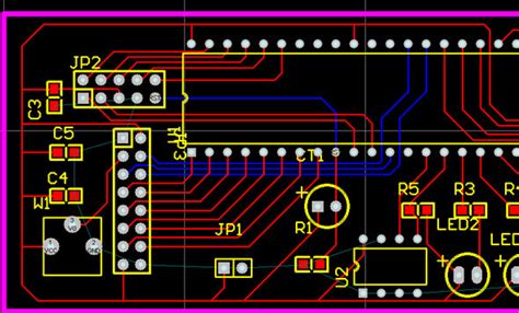
Proper component placement is essential for achieving a well-organized, manufacturable, and functional PCB. When placing components on your board, consider the following:
– Functionality: Group related components together to minimize track lengths and improve signal integrity
– Manufacturability: Ensure components are accessible for automated assembly and manual soldering
– Thermal management: Place heat-generating components away from sensitive devices and provide adequate cooling
– Mechanical constraints: Consider the physical size and shape of components, as well as any mounting requirements
By optimizing component placement, you can reduce the overall PCB size, minimize signal delays, and improve the board’s performance and reliability.
Rule 4: Use Appropriate Via Size and Placement
Vias are small holes drilled through the PCB to connect tracks on different layers. When designing vias, consider the following:
– Current carrying capacity: Larger vias can handle higher currents without overheating
– Signal integrity: Properly placed vias minimize signal reflections and distortions
– Manufacturing constraints: Minimum via size and drill hole diameter are limited by the PCB fabrication process
As a general guideline, use the largest via size possible for power and ground connections to minimize resistance and improve Thermal dissipation. For signal vias, use appropriate size and placement based on the signal frequency and impedance requirements.
Here’s a table with some common via size guidelines:
| Parameter | Minimum Value (mm) |
|---|---|
| Via drill hole diameter | 0.2 |
| Via pad diameter | 0.4 |
| Via-to-track clearance | 0.15 |
| Via-to-via clearance | 0.3 |
Note: These values are for reference only and may vary based on the specific PCB fabrication process and design requirements.
Rule 5: Implement Proper Grounding Techniques
A well-designed grounding scheme is essential for minimizing noise, reducing EMI, and ensuring the proper functioning of the PCB. When designing your ground plane and connections, consider the following:
– Ground plane: Use a solid ground plane on one or more layers to provide a low-impedance return path for signals
– Ground connections: Use multiple vias to connect ground planes on different layers and provide a low-resistance path for current
– Isolation: Separate analog and digital grounds to minimize noise coupling, and use ground slots or split planes when necessary
By implementing proper grounding techniques, you can improve signal integrity, reduce noise, and minimize the risk of EMI-related issues.
Rule 6: Follow Manufacturer’s Recommended Footprints
When creating footprints for components, it’s essential to follow the manufacturer’s recommended dimensions and tolerances. Proper footprint design ensures that components can be accurately placed and soldered during the assembly process.
To create accurate footprints, consider the following:
– Datasheet specifications: Use the manufacturer’s provided dimensions for the component body, leads, and pads
– Pad size and shape: Ensure pads are large enough for reliable soldering and small enough to avoid bridging or short circuits
– Orientation and polarity: Clearly mark the orientation and polarity of polarized components, such as diodes and electrolytic capacitors
By following the manufacturer’s recommended footprints, you can minimize the risk of assembly errors and improve the overall reliability of the PCB.
Rule 7: Implement Proper Thermal Management
Thermal management is crucial for ensuring the long-term reliability and performance of the PCB. When designing your board, consider the following:
– Power dissipation: Identify components that generate significant heat, such as power transistors and Voltage Regulators
– Thermal relief: Use thermal relief pads or spokes to improve solderability and reduce thermal stress on components
– Cooling methods: Incorporate heatsinks, fans, or other cooling solutions for high-power components
By implementing proper thermal management techniques, you can prevent overheating, reduce the risk of component failure, and extend the lifespan of the PCB.
Rule 8: Use Appropriate Solder Mask and Silkscreen
Solder mask and silkscreen are essential for protecting the PCB and providing clear markings for assembly and troubleshooting. When designing your solder mask and silkscreen, consider the following:
– Solder mask: Use a solder mask to cover exposed copper traces and pads, preventing short circuits and improving insulation
– Silkscreen: Use clear and concise silkscreen markings to identify components, pin numbers, and polarity
– Clearance: Ensure adequate clearance between solder mask openings and adjacent pads or traces to prevent bridging or short circuits
By using appropriate solder mask and silkscreen, you can improve the PCB’s aesthetics, enhance its protection, and facilitate easier assembly and maintenance.
Rule 9: Perform Design Rule Checks (DRC)
Before sending your PCB design for fabrication, it’s crucial to perform design rule checks (DRC) to identify and resolve any potential issues. DRC is an automated process that compares your design against a set of predefined rules to ensure it meets the fabrication and assembly requirements.
Common DRC checks include:
– Clearance and creepage distances
– Track width and spacing
– Via size and placement
– Hole size and spacing
– Solder mask and silkscreen coverage
By running DRC and addressing any flagged issues, you can minimize the risk of fabrication errors, reduce production delays, and improve the overall quality of the PCB.
Rule 10: Document and Communicate Effectively
Proper documentation and communication are essential for ensuring the successful fabrication, assembly, and maintenance of the PCB. When preparing your design files and documentation, consider the following:
– Gerber files: Generate accurate and complete Gerber files for each layer of the PCB, including copper, solder mask, and silkscreen layers
– Drill files: Provide separate drill files for through-holes and vias, specifying the hole sizes and locations
– Assembly drawings: Create clear and detailed assembly drawings, including component placement, orientation, and polarity
– Bill of materials (BOM): Prepare a comprehensive BOM, listing all components, quantities, and manufacturer part numbers
By providing comprehensive and accurate documentation, you can streamline the fabrication and assembly process, reduce the risk of errors, and facilitate easier maintenance and troubleshooting.
Frequently Asked Questions (FAQ)
1. What are the most common PCB design issues?
Some of the most common PCB design issues include:
– Inadequate clearance and creepage distances
– Incorrect track width and spacing
– Poor component placement and orientation
– Improper via size and placement
– Insufficient grounding and thermal management
2. How can I ensure my PCB design is manufacturable?
To ensure your PCB design is manufacturable, follow these guidelines:
– Adhere to the fabrication house’s design rules and constraints
– Use appropriate track width, spacing, and via sizes
– Follow the manufacturer’s recommended footprints for components
– Perform thorough design rule checks (DRC) before submitting your design
– Provide complete and accurate documentation, including Gerber files, drill files, and assembly drawings
3. What is the importance of proper grounding in PCB design?
Proper grounding is essential for several reasons:
– Minimizes noise and electromagnetic interference (EMI)
– Provides a low-impedance return path for signals
– Ensures the proper functioning of the PCB
– Improves signal integrity and reduces crosstalk
4. How can I optimize component placement on my PCB?
To optimize component placement, consider the following:
– Group related components together to minimize track lengths
– Place components for easy accessibility during assembly and maintenance
– Ensure proper thermal management by placing heat-generating components away from sensitive devices
– Consider the physical size and shape of components, as well as any mounting requirements
5. What are the benefits of performing design rule checks (DRC)?
Performing design rule checks (DRC) offers several benefits:
– Identifies and resolves potential design issues before fabrication
– Minimizes the risk of fabrication errors and production delays
– Ensures the design meets the fabrication and assembly requirements
– Improves the overall quality and reliability of the PCB
Conclusion
Designing a high-quality, manufacturable, and reliable PCB requires careful planning and attention to detail. By following the 10 essential PCB design rules outlined in this article, you can optimize your designs, minimize the risk of errors, and streamline the production process.
Remember to maintain proper clearance and creepage distances, use appropriate track width and spacing, optimize component placement, and implement proper grounding and thermal management techniques. Additionally, always perform thorough design rule checks (DRC) and provide comprehensive documentation to ensure the success of your PCB project.
By adhering to these guidelines and staying up-to-date with industry best practices, you can create better PCBs that meet your design requirements and exceed your customers’ expectations.
Leave a Reply