Introduction
High density interconnect (HDI) printed circuit boards (PCBs) have increasingly become critical in the electronics manufacturing industry. As electronic devices continue to get smaller and more complex, the demand rises for HDI PCBs that can accommodate higher component densities and enable miniaturization. 10 layer HDI PCBs provide capabilities that standard PCBs cannot in terms of trace widths, trace-to-trace spacing, and via diameters. This allows greater functionality in a compact footprint, making them especially desirable for mobile, wearable, IoT, automotive, and medical devices.
Choosing the right 10 layer HDI PCB manufacturer is crucial to get boards fabricated properly for your specific application needs. This article provides a comprehensive overview of 10 layer HDI PCB technology, manufacturing capabilities required, and key factors to consider when selecting a manufacturer.
What are 10 Layer HDI PCBs?
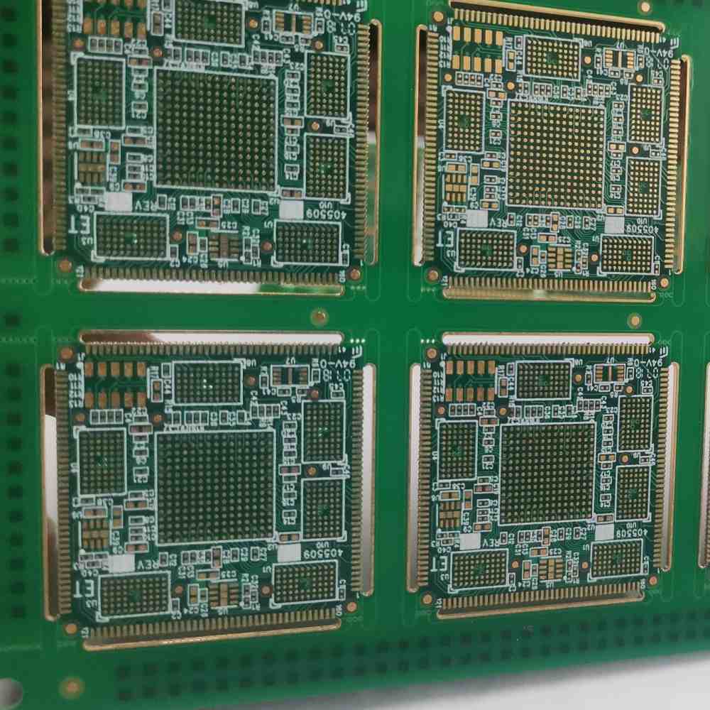
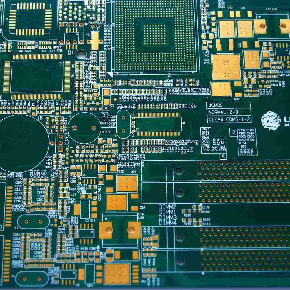
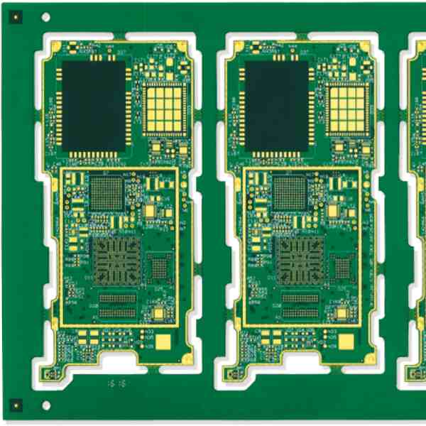
HDI PCBs use microvias and thin dielectrics to form a densely interconnected circuitry. This allows routing traces and placing components closer together than a standard PCB. 10 layer HDI PCBs consist of 10 conductive copper layers separated by dielectric material. Vias are holes that connect the traces between layers to complete circuits.
Here are some key characteristics of 10 layer HDI PCBs:
- Trace/Space Width: Can be as low as 25/25 microns (comparable to hair diameter).
- Microvia Diameter: As small as 50 microns.
- Dielectric Thickness: Can be as low as 25-50 microns.
- High Layer Count: Up to 10 layers.
- Laser Drilled Microvias: Enable connections between layers.
- Fine Line Patterning: For intricate circuitry.
- Mixed-Signal Capability: Can integrate analog and digital signals.
- High Component Density: More components packed in smaller space.
The small features and tight tolerances allow fitting more circuitry in a compact form factor necessary for many advanced electronics. The thin dielectrics between layers also enable shorter signal travel time for higher speed signals.
Why Choose 10 Layer HDI PCBs?
Here are some of the key benefits that make 10 layer HDI PCBs advantageous for certain applications:
- Miniaturization – The small features and high component density enable electronics miniaturization for portable and compact devices.
- High Speed – Thinner dielectrics mean shorter signal travel paths, allowing multi-Gbps speeds.
- Signal Integrity – Tightly spaced traces with matched impedance allow clean high frequency signal transmission.
- Higher Reliability – More solid copper layers improves thermal dissipation and reduces EMI.
- Design Flexibility – Broad routing channels and high layer count provide more options.
- Mixed Signal Circuits – Integrating analog and digital circuits reduces noise.
- Lower Costs – Miniaturization enables cost savings through less materials used.
10 layer HDI PCBs are commonly used in consumer wearables, smartphones, tablets, IoT devices, medical electronics, avionics, automotive electronics and more applications where density, speed, and reliability are critical factors. The capabilities enable improved electrical and mechanical performance in a small footprint.
10 Layer HDI PCB Manufacturing Capabilities
Producing 10 layer HDI PCBs requires advanced manufacturing capabilities and specialized processes. Here are some of the key requirements:
Fine Line Patterning
To achieve trace widths and spaces down to 25 microns, printers with high precision and registration accuracy are needed for the photolithography process. Laser direct imaging (LDI) is commonly used which can pattern down to 10 microns.
Thin Dielectrics
Dielectrics as thin as 25-50 microns are needed between layers. This calls for advanced materials like polyimides along with precision lamination presses.
Microvias
Laser drilling machines with small diameter capability are used to produce microvias down to 50 microns in size. The vias may also need to be plugged and plated.
Layer to Layer Registration
Connecting microvias between layers requires highly accurate layer to layer registration within 5 microns. This requires advanced drilling and lamination machinery.
Fine Pitch Components
Since components are packed more densely, printers and component placers with high precision are needed to populate 0201 or smaller components.
Advanced Testing
Flying probe, automated optical inspection (AOI), and X-ray inspection are used to verify minute defects in the boards given the small features. Impedance testing may also be required.
High Mix/Low Volume
The cutting edge applications often have low volume and high mix production. So changeover flexibility is key.
These are advanced capabilities that are mandatory for reliable 10 layer HDI PCB fabrication. Not all manufacturers will have these in place.
Factors to Consider for Manufacturer Selection
Here are some of the key factors to consider when selecting a 10 layer HDI PCB manufacturing partner:
Technical Capability
Can they demonstrate experience with volume production of 10 layer boards? Do they have the key machinery and process capabilities outlined earlier?
Quality Systems
Are their processes certified to quality standards like ISO 9001? Do they perform quality testing and inspection at each stage? What is their defect rate?
Customer Support
Do they have design support engineers and account managers to help optimize the board design and provide guidance? How responsive are they to technical queries?
Lead Time & On-Time Delivery
Does their lead time align with your project timeline? How consistent are they at meeting committed delivery dates? Are there provisions for expediting orders if required?
Prototyping Services
Do they have capabilities for producing prototypes in small volumes? This is key for verification before going to full production.
Advanced Services
Value-adds like assembly, conformal coating, box build, testing services help reduce the number of vendors needed and provide convenience.
Pricing & MOQ
Are their pricing models competitive and transparent? How are volume discounts structured? What is the minimum order quantity? Lower MOQs provide flexibility.
Supply Chain & Logistics
Where are they located? Do they help manage international shipping, customs, and logistics requirements?
Industry Experience
Do they have experience serving your specific industry? Familiarity with industry-specific requirements helps avoid issues.
Thoroughly evaluating manufacturers on these aspects will help identify the right partner that is qualified to produce your 10 layer HDI PCBs and can offer the complete range of services required.
Top 10 Layer HDI PCB Manufacturers
Here is an overview of some leading manufacturers of 10 layer HDI PCBs:
TT Electronics
Headquartered in the UK, TT Electronics (ttelectronics.com) is a global provider of engineered electronics for performance critical applications. They have extensive capabilities for producing high layer count, HDI boards for defense, aerospace, space, transportation, industrial, and medical applications.
AT&S
AT&S (ats.net) is Europe’s largest PCB manufacturer, headquartered in Austria. They are globally renowned for their advanced HDI PCBs using their proprietary mSAP technology. Their customers include major smartphone, automotive, and industrial manufacturers.
TTM Technologies
TTM Technologies (ttm.com) is one of the leading global PCB manufacturers based in California with plants worldwide. They offer quick-turn prototyping and volume production of multi-layer HDI boards, including for defense and aerospace.
Unimicron
Unimicron (unimicron.com) is a Taiwan-based manufacturer known for their advanced HDI and IC substrate technologies. They focus on mobile, automotive, IoT, and high speed digital applications. Their patented Apex technology enables ultra-thin HDI boards.
Tripod Technology
Tripod Technology (tripod.com.tw) is a Taiwan based manufacturer specializing in producing HDI boards for communication, automotive, industrial, and medical applications. They utilize advanced technologies like mSAP and Any-Layer HDI.
Zhen Ding Tech
Zhen Ding Tech (zdtcorp.com) is one of the largest PCB manufacturers in the world based in Taiwan. They offer advanced PCB technologies including over 30 layer count HDI boards with microvias, blind/buried vias and embedded passives.
Compeq
Compeq (compeq.com) is a Taiwan based manufacturer providing HDI PCBs with microvia and Any-Layer technologies for networking, mobile communications, automotive electronics and other applications. Their customers include major Asian, European and US brands.
WUS Printed Circuit
WUS Printed Circuit (wusgroup.com) is a Chinese PCB manufacturer offering advanced HDI boards, IC substrates, and rigid-flex PCBs. They manufacture for mobile phone, communications infrastructure, automotive, IoT and other segments.
Shennan Circuits
Shennan Circuits (szshennan.com) is a leading Chinese PCB manufacturer known for their advanced HDI PCBs using A-SAP andother proprietary technologies. They produce high layer HDI boards for smartphone, 5G, automotive, industrial segments.
Cicor
Headquartered in Switzerland, Cicor (cicor.com) provides EMS and sophisticated PCB solutions globally with sites in Europe and Asia. They manufacture HDI PCBs for medical, industrial, aerospace, defense, and communications applications.
This gives an overview of some of the top manufacturers that have demonstrated capabilities for high volume production of advanced 10 layer HDI PCBs using the latest fabrication technologies. Each has their strengths in different geographic regions and application segments.
Frequently Asked Questions
Here are some common questions about 10 layer HDI PCB manufacturing:
What are the key challenges in manufacturing 10 layer HDI PCBs?
Some key challenges include achieving very fine line widths and spaces down to 25 microns, laser drilling microvias tight tolerances, thin dielectrics of 25-50 microns, high layer count lamination registration within 5 microns, and reliable plating of microvias. This requires significant investments in advanced equipment and process engineering.
Why is laser drilling preferred over mechanical drilling for HDI boards?
Mechanical drilling struggles to reliably produce microvias below 100 microns in diameter. Laser drilling using YAG, CO2, excimer lasers can drill holes down to 50 microns or less. Lasers also produce better hole wall quality without burrs.
How do you test HDI PCBs?
Flying probe testing is commonly used. It can accurately test boards with fine traces and spaces that are challenging to test with fixtures. Other key tests are automated optical inspection, x-ray inspection, impedance testing, and functional testing of any assembled boards.
What design for manufacturing guidelines should be followed?
Use minimum trace widths and spaces specified by manufacturer. Provide adequate thermal relief pads for microvias. Maintain maximum aspect ratio on microvias. Follow other IPC guidelines like proper annular rings on microvias. Eliminate acute angles.
What type of materials are used as dielectrics?
Thin core materials used include high Tg epoxy, polyimide, PTFE composites, liquid crystal polymer (LCP), and others. Build-up films include thermoset or thermoplastic acrylics, polyimides, modified epoxies. The choice depends on electrical, thermal, mechanical needs.
Conclusion
10 layer HDI PCBs enable greater miniaturization, higher speeds, improved reliability, and enhanced performance for advanced electronics. Manufacturing them requires stringent process controls and advanced equipment capabilities to meet the tight tolerances and high densities. Partnering with an established manufacturer having certified quality systems and a proven track record of delivering such boards is key. This article has provided an overview of 10 layer HDI PCB technology and manufacturing considerations, along with profiling some of the top manufacturers in the field. Companies can leverage this information to make an informed decision when sourcing 10 layer HDI PCBs for their products.


Leave a Reply